Product & Service
Stress Station
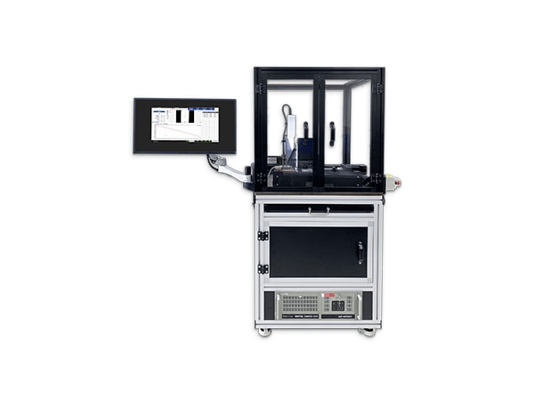
New measurement trend in wafer bending:
According to ITRS and Intel’s CMOS process technology, stress technology has become one of the key technologies in advanced nano-meter CMOS process including 90nm and beyond. This stress station is capable of stress measurement in the CMOS component and measurement of Piezo-resistance simultaneously. Similarly, this stress station is applicable to many research fields such as nano-wire, nano-tube, FinFET, GaAs component, SiGe channel component, Ge channel component, MEMS, LED, OLED, and PV.
Features:
- Direct measurement of the sample’s strain.
- Intuitive mechanism design in wafer bending jig for easy operation.
- Measurement results used in published international SCI journal paper.
- Adjustable single axial-direction stress provided by designed bending jig. (Including tension and compression)
- Augmentable to include I-V measurement and low frequency noise
| Interface | USB 2.0 | Max. sample size | 80×100 mm |
| Measurement range | 300 Mpa*1 | adjustable span range in applied force | 95 mm |
| Stress resolution | 0.05 Mpa | Pitch in span adjustment | continuous adjustable |
| Stress type | tension or compression | Dimension (length×width×height) | 240×210×195 mm |
| Young’s modulus measure | Supported | Weight | 5 Kg |
| Real-time stress calculation | Supported | Operating temperature | -20 ~ +60℃ |
| Real-time displacement analysis | Supported (Optional) | Standard Accessory | Calibration sample, Software CD, USB cable, |
| Stress and applied force measure | Supported | Language | English |
| Max. applied force | 100 N | PC Requirements | CPU:P4, HD:1GB, USB 2.0 |
| Max. stroke of applied force | 3 mm | Monitor Requirements | 1280*800 resolution |
| Adjustment of applied force | simultaneously | O.S. Supported | Windows XP, WIN 7, WIN10 |
If you are interesting this products, please download the catalog now. A sales representative will contact with you as soon as possible
© 2019 Chief SI INC. - Design By Armlet